
Privacy statement: Your privacy is very important to Us. Our company promises not to disclose your personal information to any external company with out your explicit permission.
COB encapsulation has gradually matured in the field of LED display applications, especially in the field of outdoor small pitch with its unique technical advantages. Especially in the last two years, with the improvement of production technology and production technology, COB packaging technology has made a qualitative breakthrough. Some factors that have constrained development in the past have also been solved in the process of technological innovation.
So, where are the advantages of COB packaging technology and what are the differences between it and traditional SMD packaging? Will it replace SMD as the mainstream of LED display in the future?
In general, whether a packaging technology has vitality is to see the tail (customer application) from the head of the industry chain (LED chip). Through a comprehensive analysis to assess. Among them, the final judgment right of a certain packaging technology must come from the client application, not a certain link in the industry chain. This paper will analyze and compare two package types: COB and SMD, and discuss the best package form in the field of LED display.
In general, the COB package and SMD package stand on the same starting line in the selection of LED chips, and then chose a different technology route.
First, analysis and evaluation of packagingDifferent technologies
In COB packaging, the LED chip is directly fixed on the pad of the PCB lamp bead with a conductive adhesive and an insulating adhesive, and then the LED chip is turned on. After the test is completed, it is encapsulated with an epoxy resin.
In the SMD package, the LED chip is fixed on the pad of the lamp bead by using a conductive adhesive and an insulating adhesive, and then the same conduction performance as the COB package is used for welding. After the performance test, the epoxy chip is encapsulated with an epoxy resin, and then the light is split. Cutting and playing tape, transport to screen factory and other processes.
2. Comparison of strengths and weaknesses
It is no doubt that the SMD packaging plant can produce high-quality lamp beads, but the production process is too costly. It will also increase the cost of transportation, material storage and quality control from the lamp bead assembly plant to the screen factory.
SMD believes that the COB packaging technology is too complex and that the once-through rate of the product is not well controlled by a single lamp, even an insurmountable obstacle. The failure point cannot be repaired and the yield is low.
In fact, COB packaging is based on the current level of equipment technology and quality control, 0.5K integration technology can achieve a one-time pass rate of about 70%, 1K integration technology can reach about 50%, 2K integration technology can make this The index reached about 30%. Even if there is a module that does not pass the single pass rate test, the defective point of the whole board is 1-5 points, and there are few modules with more than 5 bad points. After passing the test and repair, the qualified rate of the finished product can be improved. It reaches about 90%-95%. With the advancement of technology and the accumulation of experience, this indicator will continue to increase. At the same time, we also have a point-by-point repair technology after sealing the glue.
3. Technical analysis and evaluation
Technical Analysis Evaluation Form

Analysis and evaluation instructions:
Technical difficulty:
SMD package: It is obvious that this kind of single lamp bead single packaging technology has accumulated many years of actual combat experience, each has unique skills, but also has scale, mature technology, and it is relatively easy to implement.
COB package: It is a new packaging technology with multiple lamp beads integrated. During the practical process, many technical experiences in production equipment, production process equipment, test and test methods are accumulated and verified in constant innovation practice, and the technical threshold is high. High difficulty. The biggest difficulty currently facing is how to increase the once-through rate of products. COB packaging is faced with a technological peak, but it is not insurmountable, but it is relatively difficult to achieve.
Factory failure rate control level:
Both the COB and SMD packages can be controlled very well and can be guaranteed to fail when delivered to customers.
Cost Control:
Theoretically speaking, the cost control of COB at this stage should be slightly better, but at present the production capacity is limited, and no scale has yet been formed. Therefore, SMD is still dominant in the moment.
Reliability risks:
The square or hexagonal bracket used in the SMD package brings technical difficulties and reliability risks to the subsequent production process. For example, the lamp beads surface reflow soldering process needs to solve a large number of stent pin soldering yield problems. If SMD is to be applied outdoors, it is also necessary to solve the outdoor protection yield problem of the bracket pins.
The COB technology is due to the elimination of this bracket, and there will hardly be much technical difficulties and reliability risks in the subsequent production process. Only two technical hills are faced: one is how to ensure that the IC driver chip surface does not show a failure point on the lamp bead surface after reflow, and the other is how to solve the problem of ink consistency of the module.
Second, the reflow soldering link analysis and assessmentLamp beads surface reflow soldering process
Technical difference
The COB package does not exist because it does not have a bracket.
SMD packaging is the purchase of SMD packaging factory lamp beads by the display factory, and then patch processing to the PCB board.
2. Some questions
A. Competition issues
This link is different from the packaging link, and the packaging link is in the middle reaches of the industrial chain. There are only a handful of companies and there will be some profit margins. The screen factory is located downstream in the SMD industry chain, with many companies, relatively low technical thresholds, fierce competition, thin profits, and large pressures for survival. Among the numerous screen manufacturers, companies listed through financing have a dominant position based on financial strength, brand advantages, and advantages of foreign market channels. Other SMEs that do not have differentiated products can only make waves. The uneven development level of an enterprise will inevitably lead to an increase in the differentiation of product quality. In what kind of environment do companies do and how?
In order to do a good job at this link and minimize the problem of declining product reliability, the technology used seems simple, but it is not. The following three factors are worth our attention?
PCB board design quality, material, production process, process and storage quality control level.
SMT equipment accuracy and SMT production process quality control level.
In the face of market competition, managers' cost consciousness and quality consciousness.
We believe that competition to reduce the quality of raw materials and sacrificing product quality will have disastrous consequences for the industry chain.
B. Product Cost Issues
COB package does not have this procedure, the cost on this link is always zero.
SMD packaging As the density of product points increases, patch technology becomes more difficult and the cost of the product increases. In addition, the higher the dot density, the more the cost increases and the non-linear acceleration of the growth relationship.
C. Reliability issues
The COB package does not have this process, and there is no problem of reduced reliability at this stage.
In the SMD package, there are generally four soldering legs per bracket, and there must be a problem of reduced reliability at this stage. This is determined by reliability theory. According to the principle of reliability, the fewer control links a product has, the higher the reliability. Please see the following table:
Comparison of Quality Control Links between COB Package and SMD Package for Module Lamp Bead Reflow Process
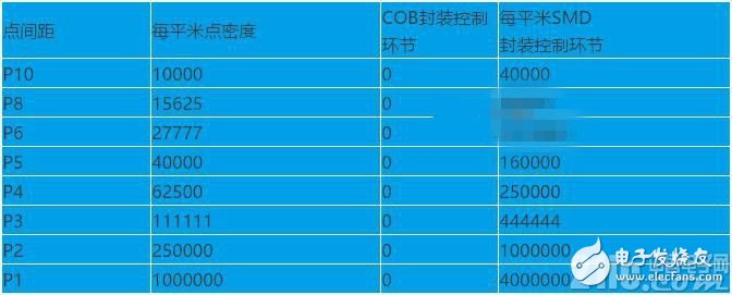
From the table, we can clearly see the fact that with the decrease of the dot pitch and the increase of the dot density, the control of the lamp bead surface is always 0, and the SMD package becomes smaller as the dot pitch becomes smaller. As the density of dots increases, its control per square meter increases by a factor of 4 with a corresponding increase in density per square meter.
D. Lamp Bead Failure Caused by Reflow Temperature
SMD lamp beads usually require about 240 degrees of temperature during reflow soldering, and lead-free soldering even reaches furnace temperatures of 260-280 degrees. There are two kinds of failure possibilities for the lamp bead device when it passes through the reflow soldering machine.
One type of failure is the risk of cracking and chipping of LED chips under high temperature: LED chips are like humans. There are also normal and abnormal individual differences. When weak and disabled individuals pass the high temperatures, they will not stand the test. Problems. If it fails immediately after passing the furnace, the problem is not great. Replace it. The fatal problem is that after the furnace has passed, the hidden danger can still be lighted. It can also pass the burn-in test, transport the shock, or expire after being used by the client for a period of time.
Another failure is the breakage failure of the LED chip solder wire.
E. The friendliness of the application process
COB encapsulated lamp beads are epoxy resin solid sealed on the PCB board, epoxy resin and PCB board affinity is very strong, with the following physical properties:
Compressive strength: 8.4kg/mm2
Shear strength: 4.2kg/mm2
Impact strength: 6.8kg*cm/cm2
Hardness: Shore D 84
Therefore, it is not afraid of static electricity, fear of collision, shock, bending deformation, abrasion resistance, and easy cleaning. Therefore, the contact with people is friendly, not squeamish, and durable.
The SMD encapsulated lamp beads are soldered to the PCB through the pins of the bracket, and the physical strength test performance is not high. Delirious fear of touch, fear of electrostatic failure caused by touch, and contact with people is not friendly.
3. Analysis and evaluation
At this stage, the advantages of COB packaging have emerged, there is no vicious competition environment, and there are no problems with cost and reliability issues. Therefore, it is not only the concept of physical space, but also the advantages of cost and reliability.
However, SMD packaging is faced with a breakthrough in how to increase the technical yield of stent pin welding at this stage, which requires a lot of manpower, material resources, and financial resources. And as the density of dots becomes denser, the problems of cost and reliability become more and more prominent.
Third, the analysis of the process of ink processing1. Technical differences
The COB package has been plagued by ink consistency problems for a long time and can now be solved technically.
SMD packaging uses a masking process to solve ink problems.
2. Analysis and evaluation
Both packages cost roughly the same in solving the problem of ink color, and neither will have the effect of reducing product reliability.
IV. Analysis and Assessment of Outdoor Protection Processes1. Technical differences
COB packaged LED wicks have been encapsulated with epoxy resin, there is no exposed soldering feet, outdoor protection to solve the problem is only the PCB board protection and waterproof structure design, technology is very simple.
A. PCB board protection
There are two levels of protection.
General outdoor application grades (such as leasing and fixing): Three anti-paint treatment processes.
High-low temperature, humidity, salt spray environment Application level: nano coating + anti UV + three anti-paint treatment process.
B. waterproof structure design
After the COB module has undergone double-sided outdoor protection, it is not afraid of water on both sides. In order to make the power supply, driver card and driver IC in the box work in a good environment and work for a longer period of time, a fully sealed design with outdoor protection is adopted in the design of the module structure. The COB module driver IC has Silicone sealing ring seals, there are heat-dissipation aluminum plate under the sealing ring, aluminum plate is embedded and fixed in the plastic parts set, there is a layer of silicone sealing ring between the kit and the box, ensuring that no water will enter the module and the box body.

The SMD package needs to protect the mounting pins of the SMD device, especially the density above P4, and the technical difficulty is considerable.
2. Face problems
A. Competition issues
COB packaging has not yet formed a large-scale production capacity. At present, it has not yet formed a cost advantage at the P8-P10 level. At present, it is only required in sports venues and rental markets that outdoor displays and high-low temperature, humidity, and salt spray application environments are not afraid of collisions. The special application market has application advantages. The P5-P6 level is comparable to SMD. The P4-P3 or even more dense pure outdoor applications will have an absolute cost advantage. Once the production capacity is formed in the future, COB packaging will have a price advantage at all point density levels. There is currently no competition among COB peers.
SMD is facing the same competition among its peers as mentioned above. Therefore, the quality of the brackets is of vital importance. To save costs and reduce the height of the brackets, it will increase the difficulty of rubber gluing technology and lower the yield of rubber grouting. This will not only reduce costs, but also increase reliability. Lowering and gluing processing costs increase.
B. Product Cost Issues
The process cost of COB packaging is basically calculated based on the outdoor treatment cost per square meter, and has little to do with the increase of the dot density.
The cost of SMD encapsulated outdoor protection increases as the density of product points increases and the difficulty of filling techniques increases. In addition, the denser the dot density, the more the cost increases, and the non-linear acceleration of the growth relationship.
C. Reliability issues
The COB package lamp surface has been encapsulated with epoxy resin. There are no exposed chips and pins in this process. Only the outdoor protection of the PCB board is properly handled, and there is basically no problem of reduced reliability.
There are 4 soldering feet for each bracket of the SMD encapsulated lamp surface, which needs to be encapsulated. Therefore, there is a yield indicator for the encapsulation of the bracket pins. As with reflow soldering, there is a problem of reduced reliability due to the bracket pins at this stage. According to the principle of reliability, the fewer control links a product has, the higher the reliability. Please see the following table:
Comparison of the Quality Control of COB Package and SMD Package of Module Lamp Bead Surface Outdoor Protection Process
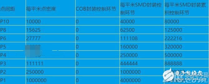
From the table, we can clearly see the fact that with the decrease of the dot pitch and the increase of the dot density, the control of the lamp bead surface is still 0, and the SMD package becomes smaller with the dot pitch. As the density of dots increases, its control will continue to increase by 4 times with the corresponding dot density. Cumulative control links refer to the accumulation of SMD's reflow process control links and gluing process control links. From the data in the table, it can be seen that this value increases by an 8-fold increase with the dot density. In an over-competitive environment, the height of outdoor SMD lamp bead holder pins is continuously decreasing, which further increases the difficulty of implementing this technology. How to fill the glue in such a tiny height of space, cover all the pins, and control the level of the module, is really an ultra-high difficulty level technology.
D. Problems with outdoor protection
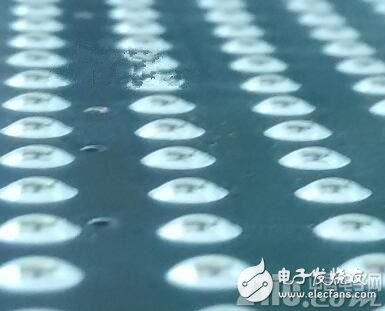
The bulb surface of the COB package is a hemispherical curve, and all devices on the lamp surface are encapsulated by epoxy resin. No device pins are exposed on the outside, and the curve is too sleek and angular. If spraying technology is used, no dead angle can be dealt with regardless of electrostatic adsorption principle or vacuum vapor deposition principle. Therefore, no matter whether it is used in indoor or outdoor environments or in harsh environment of high and low temperatures, humidity, and salt fog, there will be no lamp bead failure due to oxidation of the device pins. The COB package PCB board must be a gold-immersed process to ensure that the device is not easily oxidized during the entire process, thus ensuring that there are no potential oxidation hazards of the device pins when the front and back sides of the PCB are sputtered.
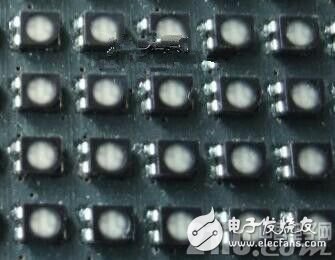
SMD encapsulated lamp beads have a large number of raised cubes with sharp corners. The bare leg of the lamp bead surface needs to be protected by outdoor protection. If indoor lamp beads are to be used for semi-outdoor use, especially in wet and salt spray environments, it must be sprayed. If the PCB board uses a spray tin manufacturing process, the device pins are prone to oxidation hazards during the manufacturing process, and then the sputtering is performed, and the effect is not satisfactory. There is a dead zone in the shaded area below the belly of the lamp.
3. Analysis and evaluation
At this stage, the advantages of the COB package reappear, and there is no problem of reduced reliability. At present, outdoor technology has broken through to the P3.0 level.
SMD packaging continues to face the technical problem of how to increase the yield of the outdoor protection of the mounting bracket pins at this stage. For outdoor small distances, the technical difficulty is even greater. It takes a lot of manpower, material resources and financial resources to break through this technology. And as dot density becomes higher, cost and reliability issues become prominent.
Fifth, the end customer's reliability experienceBoth packages come to the end customer through different technical routes, and their experience is the most talked about. Theoretical analysis needs to be evaluated by their practical application.
With the constant increase of COB package display screens and the continuous expansion of special application fields, the market will definitely analyze and select these two packaging technologies. The power of this choice comes from the market, from the end of the industry chain.
Here we only give the reliability data of COB outdoor products after one year of use at the terminal client (except for the copycat COB products):
Full-color point failure rate: less than 100,000
Single-color screen failure rate: less than 8 parts per million
Conclusion:
To sum up the detailed analysis of each link, the following two charts are used to summarize the two technology styles in the LED display industry chain.
COB packaging technology:
From the beginning of packaging to the completion of display screen manufacturing, COB packaging technology is the integration of the LED display industry chain in the middle and lower reaches of the chain, all production is completed in a factory. This kind of production organization has a simple form, a compact process, higher production efficiency, and is more conducive to a fully automated production layout. This organizational form is also more conducive to the quality control of the entire product process. This form of organization is still an organic whole. In the product development stage, we must consider the problems that may be encountered in various production processes and comprehensively assess and formulate technical implementation plans. This form of organization can also better assume quality responsibility for end customers.
From the perspective of the difficulty of technical implementation and the impact on product reliability in the entire production process, it can be seen from the figure below that the white abscissa represents the main process link in the industrial chain and the process chain in the white abscissa The white bar on the node indicates technical difficulty. The red line at the top of the figure indicates the reliability change curve of the product from the packaging link to the client application. The blue line represents the technical difficulty curve in different links of the industrial chain.
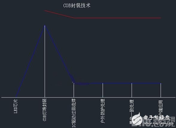
As can be seen from the figure, COB encapsulation in the field of LED displays this kind of multi-lamp integrated packaging technology is only facing a technological peak, it appears in the lamp beads encapsulation. Moreover, this technology is not insurmountable, but it is also not a reflection of everybody’s past. It is a manifestation of an integrated technology that requires countless failures and summaries of lessons learned, requires years of technical accumulation and precipitation, and requires firmness and practicality. The spirit of craftsman who is not afraid of difficulties and innovates. Once the peak of this technology is crossed, like the squid jump gantry, the road behind the mountain will be a horse flat river, there is no more technical difficulties in the entire production process. From the red product reliability curve, it can be seen that once the COB package seals the lamp beads, the subsequent production steps have little effect on its reliability. After one year of client application, reliability indicators and packaging time are almost the same.
SMD packaging technology:
The packaging companies and display companies in the SMD display industry chain are two types of independent enterprises. Industrial profits are shared by these two types of enterprises. Although the cake is large, there are many companies and the competition is fierce and the profits are thin. This kind of production organization is complex, it will waste a part of the industry's profits and efficiency, and it is relatively difficult to control product quality. Because the packaging link and the display factory link are independent from each other, it is difficult for the technical difficulties in the production process to cooperate effectively and collaboratively. Once a terminal customer uses a product with quality problems, it involves many links and it is difficult to pursue responsibility.
From the perspective of the difficulty of technical implementation and the impact on product reliability in the entire production process, the color and meaning of the curve in the following figure are the same as those in the previous figure. The figure can be seen in the SMD display packaging industry chain, there are dual-hump-style technology peaks, these two technical difficulties are appearing in the screen factory, and the packaging process due to the maturity of the technology, the technical difficulty is relatively small. Therefore, the technical difficulty of the SMD display superimposed together will definitely exceed the difficulty of COB packaging technology.
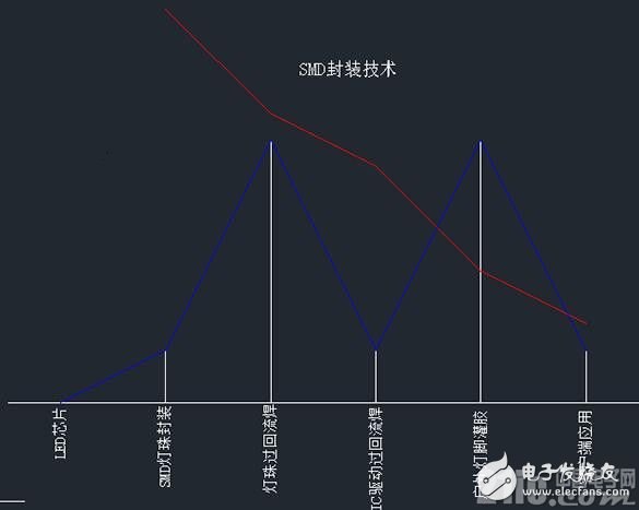
The deterioration of the competitive environment and the unbalanced distribution of profits affect the red line of product reliability starting from the packaging plant. Although the red line of each plant is high or low, the downward trend in the arrival of client applications is good. What doubts is determined by reliability theory. This is the real reason why the customer application end feels inconsistent with the product reliability and the packaging factory's factory standards. Therefore, SMD's product reliability is mainly determined by the screen factory.
In the future, in the field of display, which packaging method is more vital, I believe that the end user will make the right choice. To provide customers with cost-effective display products is the direction of COB packaging efforts, COB packaging in the product reliability and price civilians will make important contributions to the development of the industry.
November 21, 2022
September 29, 2022
August 10, 2024
April 30, 2024
Bu tedarikçi için e-posta
November 21, 2022
September 29, 2022
August 10, 2024
April 30, 2024

Privacy statement: Your privacy is very important to Us. Our company promises not to disclose your personal information to any external company with out your explicit permission.

Fill in more information so that we can get in touch with you faster
Privacy statement: Your privacy is very important to Us. Our company promises not to disclose your personal information to any external company with out your explicit permission.